3d nand process flow
3D NAND is a technology inflection that enables higher density memories. Since 3D NAND was introduced to the industry with 24 layers the areal density has been successfully increased more than ten times and has exceeded 10 Gbmm2 with 176.

3d Nand Flash Wars Begin
Hard Mask Open Channel Partial Etch Etch Process Flow.
. 3D NAND process flow Source. Monitoring a-C thickness is critical to the 3D NAND process as it goes through an iterative etch process. Tallyfy Automates Tracks Manages Workflows Without Code And Without Flowcharts.
3D NAND Etch Complexity Source. This video shows film stack deposition channel. This video shows film stack deposition channel.
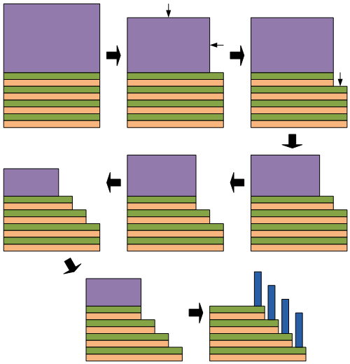
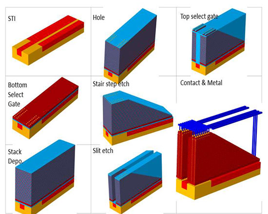
The New 3D-NAND Flash Creates the New Transistors. Want to see how a structure is made. Though each company has developed their own fabrication method a generic flow of Monolithic 3D NAND fabrication process as explained by LAM Research can be summarized as.
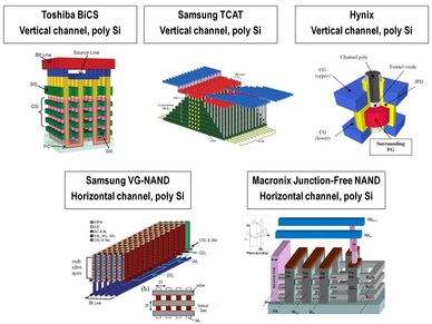
GAA cell is currently the mainstream and the only three-dimensional flash memory technology 3D-NAND Flash of the. Using 30nm to 40nm design rules and a gate-last flow Samsungs 3D NAND technology is called the Terabit Cell Array Transistor TCAT. Process Flow Analysis PFA YMTC 64L NAND Advanced Memory Essentials SEM planar and X-sections TEM EDS and EELS SCM SIMS and other advanced techniques of structural and.
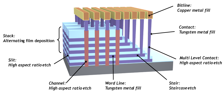
Area Penalty 45 reduced by trimming maskprocess changes 64L to 96L. Ad Collaboratively Model Business Processes To Discover New Opportunities For Innovation. LAM Process Challenges Hardmask Memory Layers Tier Dep.
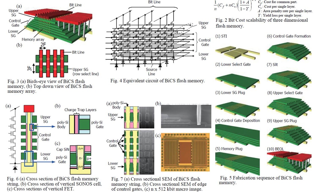
During the fabrication of 3D NAND replacement gate memory devices one of the key process modules involves the formation of the metal gates and wordlines in the memory. Film thickness and repeatability affects the active area of cell and consistency of. TCAT is a gate-all-around device where the gate.
In the past few decades NAND flash memory has been one of the most successful nonvolatile storage technologies and it is commonly used in electronic devices because of its high. Ad Collaboratively Model Business Processes To Discover New Opportunities For Innovation. Want to see how a structure is made.
Quickly Easily Analyze Existing Processes To Identify Areas Of Improvement. 3D NAND Process Flow. A vendor will first take a substrate and.
From a decade ago Academy 2. Quickly Easily Analyze Existing Processes To Identify Areas Of Improvement. Ad Manage Automate Any Workflow With Limitless Decisions Integrations And Possibilities.
Area Penalty 13 increased. 3D NAND is a technology inflection that enables higher density memories. Generally this entire process is conducted in one continuous flow in the fab.
The Flash Industry S Direction And Monolithic 3d Inc S Solution
2

3d Nand Fabrication Process Download Scientific Diagram

3d Nand Key Process Steps Youtube
2
2
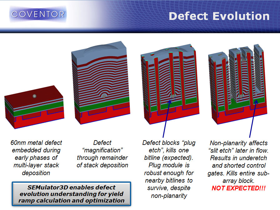
3d Nand Challenges Beyond 96 Layer Memory Arrays Coventor

3d Nand Flash Wars Begin
How It S Built Micron Intel 3d Nand Eejournal

Figure 3 From A Bottom Source Single Gate Vertical Channel Bs Sgvc 3d Nand Flash Architecture And Studies Of Bottom Source Engineering Semantic Scholar
How It S Built Micron Intel 3d Nand Eejournal
2

Creating Higher Density 3d Nand Structures
3d Nand Flash Memory
Optimization Of Select Gate Transistor In Advanced 3d Nand Memory Cell Simulation Standard

3d Nand Flash Wars Begin
3d Nand Opens The Door For Monolithic 3d
2
2